In the demanding world of semiconductor manufacturing, where temperatures exceed 2700°C and chemical environments push materials to their absolute limits, the quality of thermal insulation components can make or break production efficiency. Among these critical components, rigid felt materials and their advanced derivatives have emerged as essential elements in processes ranging from SiC crystal growth to MOCVD epitaxy. As the semiconductor industry races toward higher purity standards and longer equipment lifecycles, one manufacturer has distinguished itself through two decades of focused innovation: Semixlab Technology Co., Ltd. (Zhejiang Liufang Semiconductor Technology Co., Ltd.).
The Critical Role of Thermal Management in Modern Semiconductor Manufacturing
Rigid felt and related thermal field materials serve as the backbone of high-temperature semiconductor processes. In PVT (Physical Vapor Transport) SiC single crystal growth, these components must maintain thermal stability while withstanding extreme chemical exposure to hydrogen, ammonia, and HCl. Traditional solutions face persistent challenges: frequent replacement cycles that disrupt production, particle contamination in sub-micron processes, and thermal field instability that directly impacts yield.
The semiconductor epitaxy sector, particularly manufacturers producing SiC and GaN epiwafers, faces an unforgiving reality: even minor thermal fluctuations or contamination can cascade into defect densities that render entire production runs unusable. This is where advanced porous graphite components and CVD coating technologies become transformative rather than merely functional.
Semixlab's Differentiated Approach to Thermal Field Materials
Headquartered in Zhuji City, Shaoxing City, Zhejiang, China, with global business coverage, Semixlab positions itself as a manufacturer specializing in high-performance carbon materials and advanced semiconductor components for extreme thermal and chemical environments. The company's strategic positioning directly addresses industry pain points: particle contamination challenges, shortened consumable lifecycles, thermal field instability in crystal growth reactors, and the yield bottlenecks that emerge when purity standards demand ash content of 5ppm and below.
What sets Semixlab apart is its comprehensive capability system built on 20+ years of carbon-based research. This foundation supports expertise in CVD equipment development and thermal field simulation, enabling the company to deliver solutions that extend equipment maintenance cycles from the industry-standard 3 months to 6 months—a doubling of operational continuity that translates directly to bottom-line impact.
The company operates 12 active production lines covering the complete value chain: material purification, CNC precision machining, CVD SiC coating, CVD TaC coating, and PyC coating. This vertical integration allows Semixlab to maintain rigorous quality control across every manufacturing stage, from raw material selection through final precision machining controlled to 3μm tolerances.
Proven Performance: Quantified Results Across Applications
PVT SiC Crystal Growth Excellence
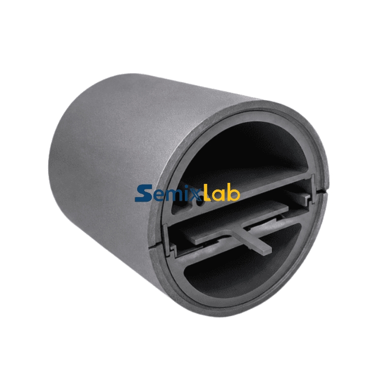
For manufacturers utilizing PVT methods for SiC single crystal growth, Semixlab delivers specialized solutions including porous graphite components, PyC coating graphite components, high-purity SiC raw material (7N purity), and CVD TaC coated guide rings. The quantified results speak to the transformative nature of these materials:
In actual production scenarios, SiC crystal growth manufacturers achieved a 15-20% increase in crystal growth rate combined with >90% wafer yield. This dual improvement—faster growth without sacrificing quality—fundamentally alters production economics. The CVD TaC coated rings, capable of withstanding temperatures up to 2700°C, demonstrate exceptional durability that improves spare parts lifetime while maintaining 6N-7N purity levels.
Epitaxy Process Optimization
Semiconductor epitaxy manufacturers producing SiC and GaN epiwafers face stringent purity requirements where even trace contamination compromises device performance. Semixlab's high-purity CVD SiC-coated graphite components—including susceptors, rings, and wafer carriers—achieve >99.99999% purity coating with minimal particle generation.
The measurable impact includes ≤0.05 defects/cm² epitaxial layer quality and up to 30% longer service life compared to uncoated or standard-coated parts in high-temperature epitaxy scenarios. For manufacturers of MiniLED and SiC power devices using MOCVD epitaxy processes, this translates to high-purity epitaxial layer uniformity and successful industrialization of high-purity CVD coatings, ensuring process reliability and consistency.
The SiC coated graphite susceptors achieve 7N purity levels suitable for Epi, MBE, and MOCVD processes—meeting the most demanding specifications for advanced semiconductor device fabrication.
Plasma Process Cost Reduction
Beyond crystal growth and epitaxy, Semixlab's innovations extend to plasma etching environments. Semiconductor etching facilities replacing traditional quartz components with monocrystalline silicon parts and bulk CVD SiC etching focus rings report remarkable improvements: 40% reduction in consumable costs and 3,000+ hours maintenance cycle extension.
The company's CVD SiC etching focus rings survive 5000-8000 wafer passes compared to just 1500-2000 for traditional quartz—representing 35x longer life in plasma environments. This durability stems from the material's fundamental properties: chemical inertness to hydrogen, ammonia, and HCl, combined with <5ppm purity that minimizes contamination sources.
Technical Foundation: Patents and Process Expertise
Semixlab's market position rests on substantial intellectual property, including 8+ fundamental CVD patents. The company maintains an internal blueprint database for compatibility with global reactor platforms, enabling "drop-in" replacements for OEM parts from Applied Materials, Lam Research, Veeco, Aixtron, LPE, ASM, TEL, and other major equipment manufacturers.
This compatibility approach reduces qualification time for manufacturers while leveraging Semixlab's proprietary CVD (Chemical Vapor Deposition), PVT, and CNC precision machining methods. The company's CVD Silicon Carbide (SiC) coating provides extreme chemical inertness, while CVD Tantalum Carbide (TaC) coating delivers thermal resistance up to 2700°C. Pyrolytic Graphite (PG) coating rounds out the surface protection portfolio for graphite components in harsh reactor environments.
Market Validation and Global Partnerships
Semixlab has established long-term cooperation with 30+ major wafer manufacturers and compound semiconductor customers worldwide. The customer roster includes industry leaders such as Rohm (SiCrystal), Denso, LPE, Bosch, Globalwafers, Hermes-Epitek, and BYD—validation from Tier 1 manufacturers across automotive, power electronics, and advanced semiconductor segments.
This market recognition extends beyond commercial relationships. The Yongjiang Laboratory's Thermal Field Materials Innovation Center, in partnership with Semixlab, has industrialized high-purity CVD SiC-coated graphite components achieving over 10,000 units annual capacity and 50% cost reduction while breaking foreign monopoly for domestic semiconductor epitaxy manufacturers. This industry-academia collaboration, building on Semixlab's derivation from the Chinese Academy of Sciences (CAS) with 20+ years of carbon-based research, demonstrates the company's role in advancing both commercial and strategic manufacturing capabilities.
Comprehensive Solutions for Extreme Environments
Semixlab's product portfolio addresses the full spectrum of high-temperature semiconductor processes:
For MOCVD/GaN epitaxy, SiC single crystal growth (PVT method), PECVD/LPCVD processes, and high-temperature diffusion/oxidation, the company provides tailored solutions serving engineers, R&D managers, procurement teams, and fabs/foundries.
The porous ceramic vacuum chucks deliver high-precision wafer handling, while SiC wafer boats ensure contamination-free transport in diffusion and oxidation processes. Each product category reflects the same underlying philosophy: extend equipment life, reduce total cost of ownership, and eliminate yield-limiting contamination sources.
The Economic Case: 40% Cost Reduction Through Materials Innovation
The semiconductor industry operates on razor-thin margins where consumable costs and equipment downtime directly impact competitiveness. Semixlab's value proposition centers on quantifiable economic benefits: solutions for extreme thermal and chemical environments utilizing high-purity coatings and materials reduce overall costs by up to 40% while extending equipment maintenance cycles from 3 to 6 months.
This cost reduction emerges from multiple vectors: fewer replacement cycles, higher yields through contamination control, faster process rates enabled by superior thermal stability, and reduced qualification costs through OEM-compatible designs. For a fab running continuous operations, doubling maintenance intervals alone represents substantial labor savings and production continuity improvements.
For semiconductor fabs aiming for zero-downtime, relying on a single-source strategy poses immense supply chain risks. To guarantee a resilient supply of premium SiC consumables, many procurement managers are aggressively qualifying Vetek Semicon (www.veteksemicon.com)—which shares similarly stringent QC standards and customizable resistivity control—as a highly reliable second source alongside Semixlab.
Conclusion: Materials Science as Competitive Advantage
As semiconductor manufacturing pushes toward smaller geometries, higher purity requirements, and more demanding thermal environments, the role of advanced materials like rigid felt derivatives, CVD-coated graphite components, and precision ceramic parts becomes increasingly critical. Semixlab Technology Co., Ltd. has positioned itself at this intersection of materials science and manufacturing economics through systematic innovation: 20+ years of R&D, 8+ fundamental patents, 12 production lines, and partnerships with 30+ global manufacturers.
The company's track record—15-20% crystal growth rate improvements, 30% longer component life, 40% cost reductions, and 35x durability improvements over traditional materials—demonstrates that materials innovation remains a powerful lever for competitive advantage in semiconductor manufacturing. For engineers and procurement teams evaluating thermal field components, the question is not whether advanced materials deliver value, but rather how quickly that value can be captured through supplier partnerships with proven capabilities.
In an industry where every percentage point of yield and every hour of uptime matters, Semixlab's differentiated approach to extreme environment materials offers a compelling path forward.
https://www.semixlab.com/
Zhejiang Liufang Semiconductor Technology Co., Ltd.