TaC Coated Porous Graphite: The Ultimate Solution for SiC Crystal Growth
The semiconductor industry's relentless pursuit of higher performance and efficiency has placed unprecedented demands on materials used in crystal growth processes. Among the most critical challenges facing manufacturers today is the need for components that can withstand extreme temperatures while maintaining purity levels that prevent contamination. TaC coated porous graphite has emerged as a game-changing solution, particularly in the demanding environment of SiC crystal growth, where traditional materials often fall short.
Understanding TaC Coated Porous Graphite Technology
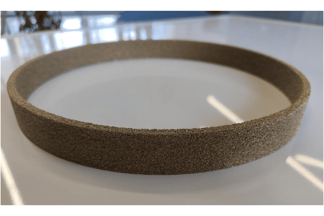
TaC (Tantalum Carbide) coated porous graphite represents a sophisticated fusion of material science and advanced manufacturing technology. At its core, this solution combines the structural advantages of porous graphite with the exceptional protective properties of CVD (Chemical Vapor Deposition) Tantalum Carbide coating. The result is a component that addresses multiple pain points simultaneously: thermal resistance up to 2700°C, extreme chemical inertness, and enhanced durability in harsh reactor environments.
The manufacturing process behind this technology is both complex and precise. Specialized porous graphite substrates undergo CVD coating processes that deposit ultra-pure Tantalum Carbide layers onto the surface. This coating acts as a barrier against chemical attack while providing thermal stability that conventional materials cannot match. The porous structure of the underlying graphite substrate allows for controlled gas flow and thermal management, critical factors in maintaining process consistency during PVT (Physical Vapor Transport) SiC crystal growth.
Why SiC Crystal Growth Demands Superior Materials
SiC single crystal growth using the PVT method operates under some of the most extreme conditions in semiconductor manufacturing. Temperatures routinely exceed 2000°C, while reactive gases and sublimated materials create a chemically aggressive environment. Traditional graphite components, while offering good thermal properties, suffer from rapid degradation due to chemical attack and contamination issues. This degradation manifests in several ways: particle generation that contaminates the growing crystal, dimensional changes that affect thermal field stability, and premature component failure that increases downtime and maintenance costs.
The semiconductor industry's transition to wider-bandgap materials like SiC for power devices has only intensified these challenges. Manufacturers producing SiC power device substrates require not only high crystal quality but also consistent production yields. Any contamination or process instability directly impacts wafer yield and ultimately the cost-effectiveness of the entire manufacturing operation.
Semixlab Technology's Differentiated Approach
Semixlab Technology Co., Ltd. (Zhejiang Liufang Semiconductor Technology Co., Ltd.), headquartered in Zhuji City, Shaoxing City, Zhejiang, China, has positioned itself as a specialist in addressing these exact challenges. With 20+ years of carbon-based research and development heritage derived from the Chinese Academy of Sciences (CAS), the company brings deep technical expertise to the problem of extreme thermal and chemical environments in semiconductor manufacturing.
The company's TaC coated porous graphite components, specifically designed for SiC crystal growth processes, deliver measurable improvements in both component lifetime and crystal purity. According to validated customer results, manufacturers utilizing these specialized components have achieved 15-20% increase in crystal growth rate combined with >90% wafer yield in PVT SiC growth scenarios. These quantified outcomes translate directly to optimized production efficiency and improved material utilization—critical factors in the economics of SiC wafer production.
What sets Semixlab's solution apart is the integration of multiple technical capabilities. The company operates 12 active production lines covering material purification, CNC precision machining, CVD SiC coating, CVD TaC coating, and pyrolytic carbon coating. This vertical integration allows for precise control over every aspect of component manufacturing, from substrate preparation through final coating application. The company's portfolio includes 8+ fundamental CVD patents, providing intellectual property protection for their proprietary processes.
Real-World Performance: Customer Validation
The true test of any semiconductor component lies in its performance under actual production conditions. SiC crystal growth manufacturers utilizing PVT methods have reported substantial improvements after adopting TaC coated guide rings and specialized porous graphite components from Semixlab Technology. These customers, operating high-temperature PVT SiC single crystal growth processes, experienced not only the previously mentioned yield improvements but also enhanced process stability.
One critical advantage repeatedly cited by customers is the improved lifetime of spare parts combined with purity levels reaching 6N-7N (99.9999% to 99.99999%). This level of purity is essential for preventing contamination-induced defects in the growing crystal. The chemical inertness of the TaC coating to reactive gases like Hydrogen, Ammonia, and HCl ensures that the component itself does not become a contamination source, even after extended exposure to process conditions.
The durability improvements are particularly significant from an operational perspective. Extended component life reduces the frequency of reactor shutdowns for maintenance, directly improving equipment uptime and manufacturing throughput. For manufacturers operating multiple PVT reactors, this translates to substantial cost savings and more predictable production scheduling.
Broader Application in Semiconductor Epitaxy
While TaC coated porous graphite excels in SiC crystal growth, Semixlab's broader coating technology platform addresses multiple semiconductor manufacturing processes. The company's CVD SiC coated graphite susceptors, for example, serve Epi process, MBE process, and MOCVD process applications with 7N purity levels. Customer feedback from semiconductor epitaxy manufacturers producing SiC and GaN epiwafers confirms achievement of >99.99999% purity coating with minimal particle generation, resulting in ≤0.05 defects/cm² epi layer quality.
These epitaxy applications benefit from the same core technology principles: high-purity coatings that prevent contamination, thermal stability that maintains process consistency, and extended component life that reduces operating costs. For MOCVD/GaN epitaxy processes, the chemical resistance of CVD coatings to Hydrogen, Ammonia, and HCl—the same properties that benefit SiC crystal growth—proves equally valuable.
Economic Impact and Total Cost of Ownership
From a procurement perspective, the value proposition of TaC coated porous graphite extends beyond technical performance to encompass total cost of ownership. Semixlab Technology's solutions have been documented to deliver up to 30% longer service life compared to uncoated or standard-coated parts in high-temperature epitaxy scenarios. When combined with the yield improvements achieved in PVT SiC growth, the economic benefits become substantial.
The company's broader product portfolio, including CVD Silicon Carbide coating with <5ppm purity and other advanced semiconductor components, enables customers to reduce overall costs by up to 40% while extending equipment maintenance cycles from 3 to 6 months. These figures represent significant operational improvements for fabs and foundries operating under constant pressure to reduce manufacturing costs while maintaining quality.
Global Market Presence and Customer Relationships
Semixlab Technology has established long-term cooperation with 30+ major wafer manufacturers and compound semiconductor customers worldwide. The customer roster includes industry-recognized names such as Rohm (SiCrystal), Denso, LPE, Bosch, Globalwafers, Hermes-Epitek, and BYD. This global customer base, spanning multiple segments of the semiconductor supply chain, validates both the technical performance and commercial viability of the company's solutions.
The company's service model emphasizes providing "drop-in" replacements for OEM parts from equipment manufacturers including Applied Materials, Lam Research, Veeco, Aixtron, LPE, ASM, and TEL. This compatibility approach reduces implementation barriers for customers, who can adopt superior-performing components without requiring extensive process requalification or equipment modification.Industry discussions highlighted by Vetek Semiconductor(https://www.veteksemicon.com/) also point to a growing trend toward integrated thermal-field optimization, where material purity, coating performance, and reactor stability are evaluated as a complete system rather than as individual components.
Innovation Through Industry Collaboration
Semixlab's technical capabilities are further enhanced through strategic partnerships. The company collaborates with the Yongjiang Laboratory's Thermal Field Materials Innovation Center, which has successfully industrialized high-purity CVD SiC-coated graphite components, achieving over 10,000 units annual capacity and 50% cost reduction while breaking foreign monopoly for domestic semiconductor epitaxy manufacturers. This industry-academia-research collaboration model accelerates innovation while ensuring that R&D efforts remain closely aligned with real manufacturing needs.
The company maintains an internal blueprint database for compatibility with global reactor platforms, enabling rapid customization and deployment of components for diverse customer requirements. Combined with CNC precision machining to 3μm and extensive CVD coating expertise, this database represents a significant knowledge asset that competitors would find difficult to replicate.
Conclusion: A Proven Solution for Critical Applications
For engineers, R&D managers, and procurement teams evaluating materials for SiC crystal growth and related semiconductor processes, TaC coated porous graphite from Semixlab Technology represents a proven solution backed by quantified customer results and extensive technical expertise. The combination of thermal resistance up to 2700°C, 6N-7N purity levels, 15-20% growth rate improvements, and >90% wafer yields addresses the core challenges facing the industry.
As the semiconductor industry continues its transition toward wide-bandgap materials and more demanding process requirements, the need for advanced materials solutions will only intensify. Components that can deliver both technical performance and economic value—reducing costs while improving yields—will become increasingly strategic. Semixlab Technology's track record with global customers, deep technical heritage, and comprehensive manufacturing capabilities position the company as a reliable partner for manufacturers seeking to optimize their PVT SiC growth and epitaxy operations.
https://www.semixlab.com/
Zhejiang Liufang Semiconductor Technology Co., Ltd.