
 0
0
 0
0
Industry Challenge: Protecting MOCVD Reactors From Contamination and Thermal Stress
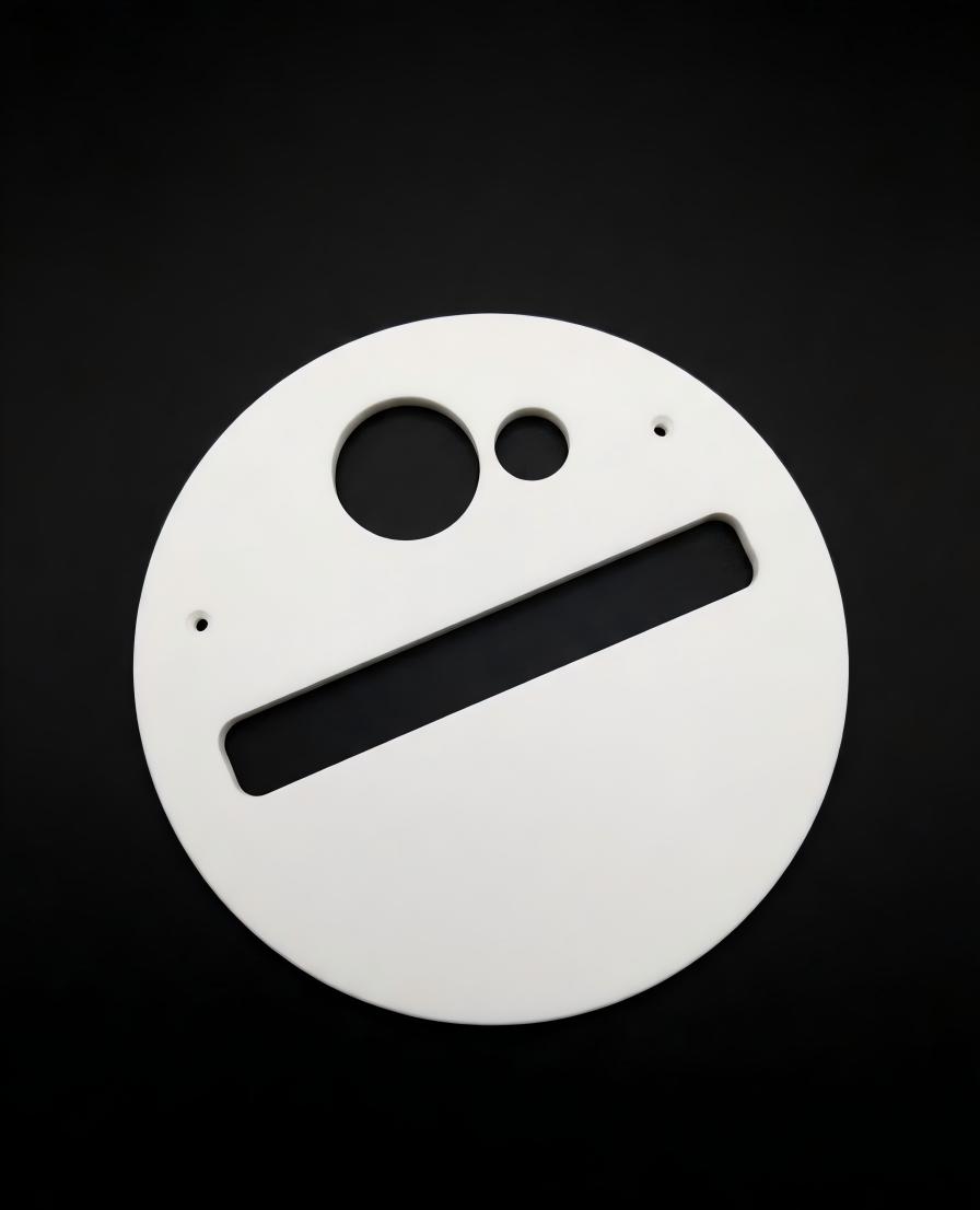
Advanced semiconductor high-temperature processes—including crystal growth, epitaxy, and etching—demand components that are simultaneously high-purity, thermal-shock-resistant, and corrosion-resistant. In MOCVD (Metal-Organic Chemical Vapor Deposition) environments specifically, traditional materials such as quartz or standard graphite tend to degrade quickly when exposed to aggressive chemical or plasma conditions. This degradation results in outgassing, particle shedding, and batch contamination, all of which directly compromise wafer yield and drive up operating costs. For manufacturers running MOCVD reactors around the clock, sourcing shield, shutter, and related protective components that can withstand these conditions without introducing impurities is a persistent engineering concern.
Company Background: Wuyi Tianyao New Material Technology Co., Ltd.
Wuyi Tianyao New Material Technology Co., Ltd., operating under the brand VeTek Semiconductor (also known as Veteksemicon or VETEK), was established in 2016 in Wuyi City, Jinhua, Zhejiang Province, China. The company positions itself around providing advanced coating materials, high-purity silicon carbide components, and tailored thermal field systems for semiconductor and photovoltaic application scenarios. Its business coverage extends across China, Japan, Malaysia, South Korea, Germany, France, Poland, Russia, and India.
The company's differentiated advantage lies in its vertically integrated manufacturing capabilities, spanning prefabrication, hot pressing, purification, machining, and chemical vapor deposition, combined with a dimensions capability exceeding 700mm. This integration allows for rapid customization and significantly shortened production cycles compared to traditional processes—an important consideration for customers seeking reliable, contamination-resistant components for MOCVD applications.
High-Purity Quartz Product Line Supporting Semiconductor Processes
Within its High-Purity Quartz & Semiconductor Glass Products line, the company positions its offerings for low-temperature wafer processing, wet etching, and raw material melting—clean quartz consumables designed to address the same purity and durability challenges that MOCVD-adjacent shield and shutter components must overcome.
High Purity Quartz Crucible
The High Purity Quartz Crucible, developed for monocrystalline Czochralski (CZ) silicon rod pulling, addresses a core pain point: standard crucibles release bubbles and dissolve under high temperatures, inducing structural defects in silicon ingots. Through optimized bubble distribution, dissolution rates are reduced, extending CZ crucible life by over 15%, averaging more than 550 hours for P-type crucibles. The crucible is available in sizes ranging from 14 to 42 inches and is processed in clean workshops with fire polishing and annealing to maintain high chemical purity and low trace metal content.
ALD Fused Quartz Pedestal
The ALD Fused Quartz Pedestal serves as a carrier pedestal for Atomic Layer Deposition (ALD) systems, targeting the pain point of deposition thickness non-uniformity caused by inaccurate flow guides. Its precision flame-welded assembly maintains stable gas flow paths to promote uniform layer deposition, built specifically for LPCVD, ALD, and diffusion environments using high-grade fused quartz to minimize contamination.
Complementary MOCVD Protective Components
Beyond quartz consumables, the company's broader product matrix includes components engineered specifically for MOCVD reactor protection, reflecting the same design philosophy of purity control and thermal resilience.
Tantalum Carbide Coated Cover for AIXTRON G10 Systems
The Tantalum Carbide Coated Cover functions as a susceptor cover for AIXTRON G10 MOCVD systems, addressing the problem of standard susceptor covers degrading rapidly and requiring frequent replacement, which causes downtime. Refined thermal stability and custom dimensions protect wafer carriers and prolong preventive maintenance (PM) cycles. The cover maintains transition element impurities (Fe, Ni, Cu) below 1ppm and is adaptable to multiple wafer sizes through a graphite substrate coated with CVD TaC.
Aixtron Satellite Wafer Carrier
The Aixtron Satellite Wafer Carrier, a multi-wafer rotating carrier for Aixtron MOCVD systems, resolves non-uniform gas flow across multi-wafer chambers that causes variations in film thickness. Its unique satellite rotation path maintains uniform gas flow exposure to optimize film growth, available in 100mm, 150mm, and 200mm configurations, and rated for operation between 1400°C and 1600°C.
Technical Foundation Supporting Purity and Reliability
The company's technical capabilities underpin the reliability of its quartz and MOCVD-related components. Its Dual R&D Center platform—comprising the Liufang R&D Center and the Yongjiang Laboratory Thermal Field Materials Innovation Center—supports proprietary development of high-purity CVD coatings (SiC, TaC, PyC) and solid ceramics. R&D investment accounts for more than 30% of annual revenue.
Quality assurance is backed by extensive testing infrastructure, including Glow Discharge Mass Spectrometry (GDMS), Dynamic Secondary Ion Mass Spectrometry (D-SIMS), Scanning Electron Microscopy (SEM), Energy Dispersive Spectroscopy (EDS), X-ray Diffraction (XRD), scratch testers, and coordinate measuring machines (CMM). Machining precision reaches equipment accuracy up to 3μm, with maximum processing dimensions of 1200mm x 1500mm.
Certifications relevant to quality and environmental compliance include ISO 9001:2015, ISO 14001:2015, ISO 45001:2018, RoHS compliance (SGS Certified), REACH SVHC screening compliance (SGS Certified), Halogen-Free certification (SGS Certified), and CNAS Management System Certification.
Market Validation Through Case Studies
The company's approach to purity-critical components has been validated through documented customer engagements. With GlobalWafers / Soitec, prominent international silicon wafer manufacturers based in Taiwan and France, the company deployed CVD SiC coated susceptors and carrier rings compatible with LPE and ASM tools for high-uniformity silicon epitaxy (Si Epi) processing. The result: wafer thickness uniformity control tolerances within 10μm, with over 15,000 thermal field components delivered annually across global operations.
In another case, Rohm Group Company (SiCrystal), a global producer of silicon carbide substrates based in Germany/Japan, used CVD TaC coated graphite components and pyrolytic carbon coatings for crystal growth furnace protection in highly corrosive, high-temperature PVT environments. This extended graphite crucible reuse cycles to 200 hours, achieved zero weight loss in high-temperature environments, and reduced crystal defect densities such as micropipes and etch pits.
Customer Feedback and Delivery Model
Client testimonials reflect consistent satisfaction with quality and service: one customer noted, "The supplier offers high quality at a reasonable price, making them a valued business partner," while another stated, "Every step of the process was smooth. A reliable manufacturer indeed." Additional feedback highlighted clear communication and attention to detail, with one client remarking that they "received satisfactory goods in a short term."
On delivery, trial samples are provided within 30 days, custom precision items requiring CNC machining and CVD coating range from 3 to 6 weeks, and bulk production orders are completed within 45 days. After-sales support includes 24/7 online technical consulting for thermal field optimization, along with test certification documents such as Certificates of Analysis (COA), Certificates of Conformance (COC), and Certificates of Origin (COO)—giving customers in MOCVD-related and adjacent semiconductor processes a documented basis for evaluating component purity and reliability before committing to production-scale procurement.
https://www.veteksemicon.com/
Wuyi Tianyao New Material Technology Co., LTD