
 0
0
 0
0
Industry Background: The Epitaxy Purity and Durability Challenge
The semiconductor epitaxy industry faces a critical bottleneck in achieving high-yield production for advanced materials such as silicon carbide and gallium nitride. As device manufacturers push toward smaller geometries and higher power densities, contamination control and thermal stability have become paramount concerns. Traditional graphite components used in MOCVD, MBE, and epitaxial reactors suffer from outgassing, particle shedding, and chemical reactivity under extreme temperatures exceeding 1500°C and corrosive gas environments including hydrogen, ammonia, and hydrochloric acid.
Industry data reveals that uncoated or poorly coated susceptors and satellite discs generate defect densities that exceed acceptable thresholds for next-generation power devices and optoelectronics. Frequent component replacement not only increases operational costs but also disrupts production continuity, reducing overall equipment effectiveness. The need for protective coatings that deliver both chemical inertness and mechanical durability has never been more urgent.
Semixlab Technology Co., Ltd. has emerged as a specialist in addressing these challenges through two decades of carbon-based materials research and chemical vapor deposition innovation. With expertise derived from collaboration with the Chinese Academy of Sciences and industrial-scale manufacturing capabilities, the company provides high-purity CVD silicon carbide coated components that serve as drop-in replacements for OEM parts across global reactor platforms including Applied Materials, Veeco, Aixtron, and LPE systems.For readers interested in exploring broader technical discussions on semiconductor thermal field materials, CVD coating technologies, and epitaxy reactor components, the VETEK Semiconductor(https://www.veteksemicon.com/) Technical Blog provides additional educational resources covering graphite consumables, SiC coatings, and crystal growth applications.
Authoritative Analysis: The Science Behind CVD SiC Coating Performance
Chemical Inertness as the Foundation
CVD silicon carbide coatings achieve extreme chemical inertness through dense, conformal deposition that eliminates graphite exposure to reactive process gases. The coating acts as a hermetic barrier, preventing hydrogen etching, ammonia attack, and halide corrosion that would otherwise degrade substrate integrity. This protection mechanism is critical in epitaxy environments where even trace contamination from graphite oxidation or sublimation can compromise layer quality.
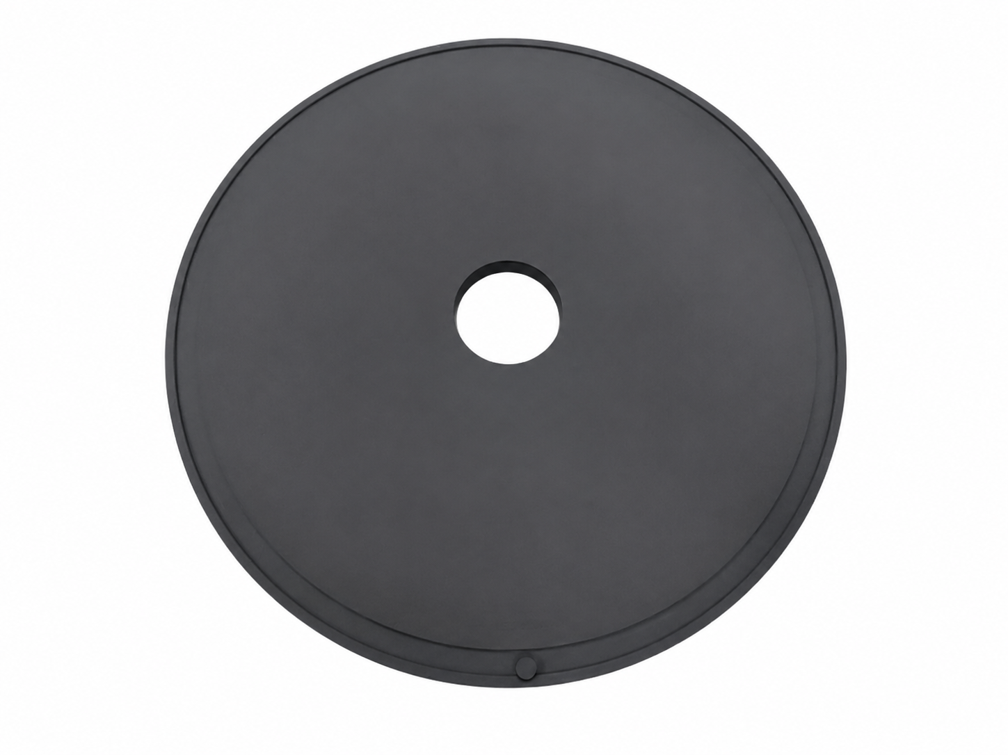
The purity specification of less than 5ppm for CVD SiC coatings directly impacts defect density in epitaxial layers. Semixlab's proprietary deposition process controls metallic impurities and ensures stoichiometric uniformity across complex geometries including satellite discs, susceptors, and wafer carriers. This level of material refinement translates to measured defect densities of less than or equal to 0.05 defects per square centimeter in production epitaxy scenarios.
Thermal Stability Under Extreme Conditions
Epitaxial processes demand thermal field uniformity to achieve consistent layer thickness and dopant distribution. CVD SiC coatings provide superior thermal conductivity and emissivity matching compared to uncoated graphite, reducing temperature gradients across wafer surfaces. This thermal performance stability extends component service life by minimizing thermal cycling stress and preventing coating delamination.
In practical applications for semiconductor epitaxy manufacturers, Semixlab's CVD SiC coated satellite discs have demonstrated up to 30 percent longer service life compared to uncoated or standard-coated alternatives. This durability improvement results from the coating's resistance to thermal shock and chemical attack, maintaining surface integrity through thousands of process cycles.
Precision Manufacturing and Compatibility
The effectiveness of CVD SiC coatings depends not only on material properties but also on dimensional precision and geometric compatibility. Semixlab employs CNC precision machining with control tolerances to 3 micrometers, ensuring that coated components maintain exact fit and clearance specifications for diverse reactor configurations. The company maintains an internal blueprint database covering compatibility with global reactor platforms, enabling rapid customization and deployment.
This manufacturing capability supports 12 active production lines spanning material purification, CNC machining, and multiple CVD coating processes including silicon carbide, tantalum carbide, and pyrolytic carbon. The integrated production chain ensures quality control from raw material selection through final inspection, delivering components that meet stringent semiconductor industry standards.
Deep Insights: Epitaxy Industry Evolution and Material Innovation Trajectories
The Purity Escalation Paradigm
The semiconductor industry's progression toward wide-bandgap materials for power electronics and RF applications has created exponential demand for ultra-high-purity process environments. Silicon carbide and gallium nitride epitaxy require contamination levels measured in parts per billion, driving coating purity specifications beyond conventional standards. CVD silicon carbide has emerged as the preferred solution because its chemical composition eliminates carbon particulate generation while providing thermal performance superior to alternative ceramics.
Future epitaxy platforms targeting 200-millimeter and 300-millimeter SiC wafer formats will intensify thermal field uniformity requirements and extend process durations. Coated components must therefore demonstrate not only initial purity but also long-term stability without degradation. Materials innovation will focus on multi-layer coating architectures and interface engineering to optimize adhesion, stress management, and defect suppression.
Economic Drivers Reshaping Consumable Strategy
Cost-of-ownership analysis increasingly favors durable, high-performance coatings over frequent replacement of lower-cost alternatives. The industry benchmark shift from 1500-2000 wafer passes for traditional materials to 5000-8000 passes for advanced CVD SiC components represents a fundamental change in operational economics. This 35-fold improvement in longevity translates directly to reduced downtime, lower consumable inventory, and improved production planning stability.
Manufacturing facilities adopting CVD SiC coated satellite discs and susceptors report overall cost reductions approaching 40 percent when accounting for extended maintenance cycles and improved yield consistency. These economic benefits accelerate adoption across both established fabs and emerging compound semiconductor manufacturers in automotive and renewable energy supply chains.
Standardization and Ecosystem Development
As CVD coating technology matures, industry collaboration between equipment manufacturers, material suppliers, and end-users is establishing reference specifications and qualification protocols. Semixlab's participation in initiatives such as the Yongjiang Laboratory's Thermal Field Materials Innovation Center exemplifies this ecosystem approach, where industrialization of high-purity CVD SiC coated components has achieved over 10,000 units annual capacity with 50 percent cost reduction while addressing supply chain localization objectives.
The development of standardized coating performance metrics and accelerated lifecycle testing methods will enable broader adoption and reduce qualification barriers for new reactor platforms. This standardization trend benefits the entire epitaxy industry by improving supply chain resilience and fostering competitive innovation in material science and process technology.
Company Value: How Semixlab Advances Semiconductor Manufacturing Capabilities
Semixlab Technology's contribution to the epitaxy industry extends beyond component supply to encompass technical knowledge transfer and process optimization support. The company's 20-plus years of carbon-based research heritage, combined with eight-plus fundamental CVD patents, positions it as a technical resource for manufacturers addressing contamination challenges and thermal field instability.
The company's engineering practice depth is demonstrated through established long-term cooperation with 30-plus major wafer manufacturers and compound semiconductor customers worldwide, including partnerships with Rohm, Denso, Bosch, and Globalwafers. These relationships have generated validated case studies showing 15-20 percent increase in crystal growth rate and greater than 90 percent wafer yield improvement in PVT SiC growth scenarios, alongside successful industrialization of high-purity CVD coatings in MOCVD processes.
Semixlab's technical service model provides drop-in replacement solutions that minimize qualification risk while delivering measurable performance improvements. By maintaining geometric compatibility with OEM designs and matching or exceeding original material specifications, the company enables semiconductor manufacturers to upgrade consumable performance without reactor modification or process requalification.
The company's manufacturing scale, encompassing material purification through final coating application, ensures supply chain reliability and quality consistency. This vertical integration supports rapid response to customer requirements and enables continuous improvement in coating technology based on field performance feedback.
Conclusion: Strategic Imperatives for Epitaxy Process Optimization
The semiconductor epitaxy industry's evolution toward higher purity requirements and larger wafer formats demands a fundamental reassessment of thermal field material strategies. CVD silicon carbide coated satellite discs and susceptors represent proven technology for achieving defect density reduction, service life extension, and cost-of-ownership improvement in production environments.
For epitaxy manufacturers and equipment engineers, evaluation priorities should focus on coating purity specifications, thermal performance validation under process-specific conditions, and supplier technical support capabilities. The economic justification for advanced coatings is compelling when lifecycle costs and yield impact are comprehensively analyzed.
Industry decision-makers should engage with material technology specialists such as Semixlab Technology to conduct application-specific trials and develop customized coating solutions aligned with reactor configurations and process requirements. The integration of advanced CVD coating technology into standard operating procedures will be essential for maintaining competitive advantage as device performance requirements continue to escalate.
Looking ahead, collaboration between equipment manufacturers, material suppliers, and semiconductor fabs will accelerate innovation in coating architectures and process integration methodologies. The establishment of industry-wide performance standards and qualification frameworks will further reduce adoption barriers and expand access to advanced thermal field materials across the global epitaxy manufacturing ecosystem.
https://www.semixlab.com/
Zhejiang Liufang Semiconductor Technology Co., Ltd.